


W11NB80 Product Details
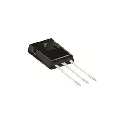
® STW11NB80 N-CHANNEL 800V – 0.65Ω – 11A – T0-247 PowerMESH™ MOSFET TYPE STW 11NB80 s s s s s s V DSS 800 V R DS(on) < 0.8 Ω ID 11 A TYPICAL RDS(on) = 0.65 Ω EXTREMELY HIGH dv/dt CAPABILITY ± 30V GATE TO SOURCE VOLTAGE RATING 100% AVALANCHE TESTED VERY LOW INTRINSIC CAPACITANCES GATE CHARGE MINIMIZED 2 1 3 DESCRIPTION Using the latest high voltage MESH OVERLAY™ process, STMicroelectronics has designed an advanced family of power MOSFETs with outstanding performances. The new patent pending strip layout coupled with the Company’s proprietary edge termination structure, gives the lowest RDS(on) per area, exceptional avalanche and dv/dt capabilities and unrivalled gate charge and switching characteristics. TO-247 INTERNAL SCHEMATIC DIAGRAM APPLICATIONS s HIGH CURRENT, HIGH SPEED SWITCHING s SWITCH MODE POWER SUPPLIES (SMPS) s DC-AC CONVERTERS FOR WELDING EQUIPMENT AND UNINTERRUPTIBLE POWER SUPPLIES AND MOTOR DRIVE ABSOLUTE MAXIMUM RATINGS Symbol V DS V DGR V GS ID ID I DM ( • ) P tot dv/dt( 1 ) Ts tg Tj Parameter Drain-source Voltage (V GS = 0) Drain- gate Voltage (R GS = 20 k Ω ) G ate-source Voltage Drain Current (continuous) at Tc = 25 C Drain Current (continuous) at Tc = 100 oC Drain Current (pulsed) T otal Dissipation at Tc = 25 o C Derating Factor Peak Diode Recovery voltage slope Storage Temperature Max. Operating Junction Temperature o Value 800 800 ± 30 11 6.9 44 190 1.52 4 -65 to 150 150 I SD ≤ 11A, di/dt ≤ 200A/µs, VDD ≤ V(BR)DSS, Tj ≤ TJMAX Un it V V V A A A W W /o C V/ns o o C C (•) Pulse width limited by safe operating area July 1999 1/8 Datasheet pdf - STW11NB80 THERMAL DATA R thj -case R thj -amb R thc-sink Tl Thermal Resistance Junction-case Max 0.66 30 0.1 300 o o o C/W C/W C/W o C Thermal Resistance Junction-ambient Max Thermal Resistance Case-sink Typ Maximum Lead Temperature For Soldering Purpose AVALANCHE CHARACTERISTICS Symbo l IAR E AS Parameter Avalanche Current, Repetitive or Not-Repetitive (pulse width limited by Tj max) Single Pulse Avalanche Energy (starting Tj = 25 o C, I D = IAR , VDD = 50 V) Max Valu e 11 500 Unit A mJ ELECTRICAL CHARACTERISTICS (Tcase = 25 oC unless otherwise specified) OFF Symbo l V (BR)DSS I DSS Parameter Drain-source Breakdown Voltage Test Con ditions I D = 250 µ A V GS = 0 Min. 800 1 50 ± 100 T yp. Max. Unit V µA µA nA V DS = Max Rating Zero G ate Voltage Drain Current (V GS = 0) V DS = Max Rating o C Gate-body Leakage Current (VDS = 0) V GS = ± 30 V T c = 125 IGSS ON (∗) Symbo l V GS(th) R DS(on) I D(o n) Parameter Gate Threshold Voltage V DS = V GS Test Con ditions ID = 250 µ A ID = 5.5 A Min. 3 T yp. 4 0.65 Max. 5 0.8 Unit V Ω Ω A Static Drain-source O n V GS = 10 V Resistance On State Drain Current V DS > ID(o n) x R DS(on )ma x V GS = 10 V 11 DYNAMIC Symbo l g f s (∗ ) C iss C os s C rss Parameter Forward Transconductance Input Capacitance Outp